| CPC H05K 9/0058 (2013.01) [H01L 23/552 (2013.01); H01L 31/167 (2013.01); H05K 9/0084 (2013.01); H05K 9/0088 (2013.01); H01L 23/60 (2013.01)] | 20 Claims |

|
1. A method for manufacturing electromagnetic shielding comprising:
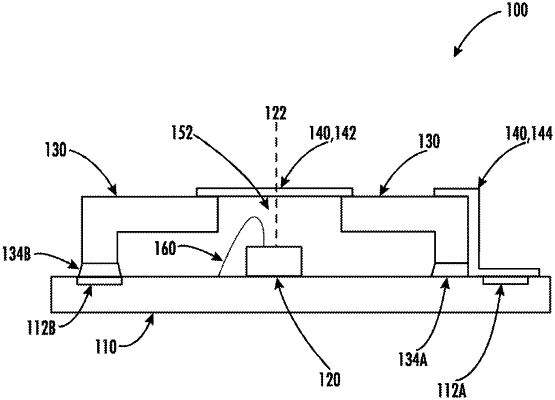
providing a substrate with an optical device attached and an RF can attached, wherein the RF can includes a first aperture aligned with an optical axis of the optical device;
depositing a deposition layer, wherein the deposition layer includes at least a first portion of the deposition layer and a second portion of the deposition layer, wherein the first portion of the deposition layer is deposited across the first aperture of the RF can and includes a second aperture that is narrower than the first aperture and aligned with the optical axis, wherein a second portion of the deposition layer is deposited on the RF can and a first terminal of the substrate, and wherein the first portion of the deposition layer and the second portion of the deposition layer are not connected;
curing the deposition layer; and
wherein the cured deposition layer electrically couples to the RF can and to the first terminal of the substrate to provide a first electromagnetic shield for at least the optical device.
|