| CPC H01Q 13/10 (2013.01) [H01Q 1/38 (2013.01); H01Q 3/34 (2013.01)] | 20 Claims |

|
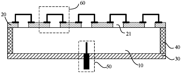
1. An antenna, comprising:
a dielectric layer having a first surface and a second surface opposite to each other in a thickness direction of the dielectric layer;
a radiating layer on the first surface of the dielectric layer, and having therein at least one slit;
a first shielding layer on the second surface of the dielectric layer, and being electrically connected to the radiating layer;
wherein the antenna further comprises:
a first insulating layer on a side of the radiating layer distal to the first surface of the dielectric layer;
at least one switch unit on a side of the first insulating layer distal to the dielectric layer, and being in one-to-one correspondence with the at least one slit; and
each switch unit comprises: a first electrode, a second insulating layer, at least one connecting portion, and a second electrode that are sequentially arranged in a direction away from the first insulating layer, wherein an orthogonal projection of the first electrode on the dielectric layer and an orthogonal projection of the second electrode on the dielectric layer overlap each other; the at least one connecting portion is connected to the second electrode to form a certain gap between the second electrode and the first electrode; and the orthogonal projection of the second electrode on the dielectric layer and an orthogonal projection of a corresponding slit on the dielectric layer at least partially overlap each other.
|