| CPC H01L 33/486 (2013.01) [H01L 25/0753 (2013.01); H01L 2933/0016 (2013.01); H01L 2933/0066 (2013.01)] | 20 Claims |

|
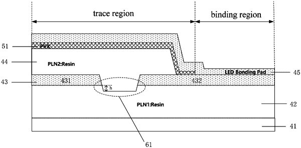
1. A displaying base plate, wherein the displaying base plate comprises:
a substrate, and a first flat layer on one side of the substrate;
a first metal layer, wherein the first metal layer is provided on one side of the first flat layer that is further away from the substrate;
a second flat layer, wherein the second flat layer is provided on sides of the first metal layer and the first flat layer that are further away from the substrate; and
a second metal layer, wherein the second metal layer is provided on one side of the second flat layer that is further away from the substrate;
wherein the first metal layer comprises a first metal trace, an orthographic projection of the second metal layer on the substrate and an orthographic projection of the first metal trace on the substrate have an overlapping part, and an orthographic projection of the second flat layer on the substrate covers the orthographic projection of the first metal trace on the substrate;
wherein the displaying base plate further comprises a passivation layer, the passivation layer is located between the second flat layer and the second metal layer, and an orthographic projection of the passivation layer on the substrate covers the orthographic projection of the second flat layer on the substrate;
wherein the first metal layer further comprises a bonding block, and the bonding block and the first metal trace are insulated and separate; and
the second metal layer comprises a trace region and a binding region that is connected to the trace region, and the bonding block is located between the substrate and the second metal layer;
wherein the binding region of the second metal layer contacts the bonding block.
|