| CPC H01L 29/87 (2013.01) [H01L 31/102 (2013.01)] | 18 Claims |

|
1. A power semiconductor component for voltage limiting, comprising:
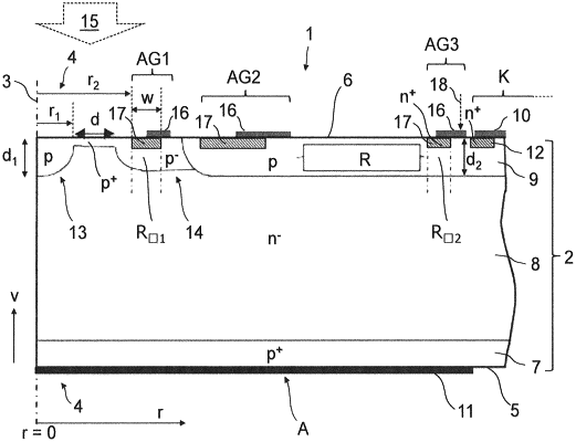
a semiconductor body in which, in a vertical direction proceeding from a rear side toward a front side opposite the rear side, a rear-side base zone of a first conduction type, an inner zone of a second conduction type complementary to the first conduction type, and a front-side base zone of the first conduction type are arranged successively,
wherein the rear-side base zone is electrically contacted with a rear-side electrode and the front-side base zone is electrically contacted with a front-side electrode,
wherein at least one switch-on structure embodied as an emitter structure of the second conduction type is embedded at least into one of the rear-side base zone and the front-side base zone and is electrically contacted by the electrode contacting the at least one of the rear-side base zone and the front-side base zone into which the at least one switch-on structure is embedded,
wherein the switch-on structure is configured to be switched on by at least one triggering structure which acts on the switch-on structure electrically via the semiconductor body and which is activatable by at least one electrical switch-on signal fed to the switch-on structure,
wherein at least one triggering structure is provided as a breakdown structure of a first type, which is designed to be activated when there is a high voltage, forming a switch-on signal of the at least one triggering structure and present between the front-side electrode and the rear-side electrode, starting from a predetermined voltage level,
wherein at least one further triggering structure is provided as a breakdown structure of a second type, which is designed to be activated when there is a high voltage, forming a switch-on signal of the at least one further triggering structure and present between the front-side electrode and the rear-side electrode, starting from a predetermined voltage gradient,
wherein the front-side electrode and the rear-side electrode are each electrically conductively pressure-contacted by an electrically conductive contact plate, such that there is in each case a contact-bonded connection or a fixed connection between the front-side electrode and the rear-side electrode and the corresponding electrically conductive contact plate, and at least one of the contact plates is embodied in such a way to function as a heat sink for dissipating heat generated in the semiconductor body out of the semiconductor body.
|