| CPC H01L 29/7848 (2013.01) [H01L 21/02532 (2013.01); H01L 21/02579 (2013.01); H01L 29/0847 (2013.01); H01L 29/1054 (2013.01); H01L 29/165 (2013.01); H01L 29/167 (2013.01); H01L 29/45 (2013.01); H01L 29/66515 (2013.01); H01L 29/66545 (2013.01); H01L 29/66795 (2013.01); H01L 29/7851 (2013.01)] | 15 Claims |

|
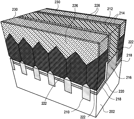
1. An integrated circuit structure, comprising:
a fin having a lower fin portion and an upper fin portion, the upper fin portion comprising germanium, and the upper fin portion having an uppermost surface;
a gate stack over the upper fin portion of the fin, the gate stack having a first side opposite a second side;
a first source or drain structure comprising an epitaxial structure embedded in the fin at the first side of the gate stack; and
a second source or drain structure comprising an epitaxial structure embedded in the fin at the second side of the gate stack, each epitaxial structure of the first and second source or drain structures comprising a first semiconductor layer in contact with the upper fin portion, and a second semiconductor layer on the first semiconductor layer, wherein the first semiconductor layer comprises silicon, germanium and phosphorous, and the second semiconductor layer comprises silicon and phosphorous, wherein the first semiconductor layer is at least partially along sidewalls of the second semiconductor layer, wherein the first semiconductor layer has an uppermost surface above the uppermost surface of the upper fin portion, and wherein the first semiconductor layer is graded from a higher concentration of germanium proximate the upper fin portion to a lower concentration of germanium proximate the second semiconductor layer.
|