|
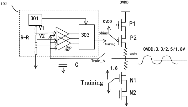
1. A driving system for detecting an on-chip voltage to adjust a gate voltage of a thin film transistor, comprising: an input circuit, configured to receive an input on-chip voltage and to output the on-chip voltage; and an adjusting circuit, configured to detect a present amplitude of the on-chip voltage output by the input circuit and to output a bias voltage corresponding to the present amplitude of the on-chip voltage to a gate of the driven thin film transistor, wherein a source of the thin film transistor is directly or indirectly coupled to the on-chip voltage, and the bias voltage is lower than the on-chip voltage, wherein the adjusting circuit has a structure selected from a group including a first structure, a second structure and a third structure: the first structure comprises: a reference voltage generator, configured to output a plurality of reference voltages related to N selectable amplitudes of the on-chip voltage; a plurality of comparators, wherein each comparator is configured to compare the on-chip voltage output by the input circuit with a corresponding reference voltage and outputs comparison results; and a decision maker, configured to determine a mode related to the present amplitude of the on-chip voltage output by the input circuit detected from N modes related to the N selectable amplitudes of the on-chip voltage based on the comparison results of the plurality of comparators, and to output a bias voltage corresponding to the mode to the gate of the driven thin film transistor according to the determined mode, wherein N is a positive integer greater than 1, the second structure comprises: a V/I and I/V conversion circuit, configured to output a corresponding bias voltage based on the on-chip voltage output by the input circuit according to an input-output relationship between the on-chip voltage and the bias voltage, wherein the V/I and I/V conversion circuit comprise: a V/I conversion circuit, configured to convert the input on-chip voltage into a current signal; and a I/V conversion circuit, configured to convert the current signal into the corresponding bias voltage, and the third structure comprises: a plurality of resistors, configured to divide the input on-chin voltage to output a divided voltage.
|
