| CPC H01L 29/41733 (2013.01) [H01L 27/0886 (2013.01); H01L 29/42392 (2013.01); H01L 29/7851 (2013.01); H01L 29/78696 (2013.01)] | 19 Claims |

|
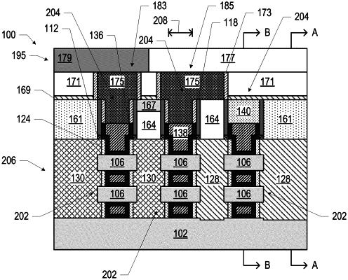
1. An integrated circuit (IC) structure, comprising:
a first source/drain (S/D) contact over a first S/D region of a transistor device;
a gate contact, wherein the gate contact is in contact with a gate and with the first S/D contact; and
a second S/D contact over a second S/D region of the transistor device, the second S/D region and the first S/D region on opposite sides of the gate, wherein a height of the second S/D contact is less than a height of the first S/D contact.
|