| CPC H01L 29/0696 (2013.01) [H01L 29/0808 (2013.01); H01L 29/0821 (2013.01); H01L 29/1008 (2013.01); H01L 29/6625 (2013.01); H01L 29/735 (2013.01); H01L 29/408 (2013.01)] | 20 Claims |

|
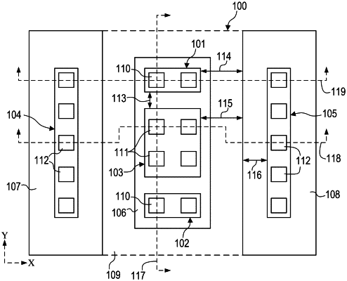
1. A transistor tile formed within a horizontal length, a horizontal width, and a vertical thickness, the transistor tile comprising:
a first PLDD region formed as a first collector region located within a first portion of the transistor tile;
a second PLDD region formed as a second collector region located within a second portion of the transistor tile;
an N-well formed as a base region located within a central portion of the transistor tile between the first and second PLDD regions, wherein the central portion is horizontally between the first and second portions, and a direction of a flow of a base-collector current is horizontal between the first and second collector regions and the base region; and
an emitter P+ region formed as an emitter region located within the central portion of the transistor tile and in the N-well, wherein a direction of a flow of a collector-emitter current is horizontal between the first and second collector regions and the emitter region, and a direction of a flow of a base-emitter current is horizontal through the base region;
wherein the direction of the flow of the base-emitter current is perpendicular to the direction of the flows of the base-collector current and the collector-emitter current.
|