| CPC H01L 27/14605 (2013.01) [H01L 27/14616 (2013.01); H01L 27/14658 (2013.01); H01L 27/14689 (2013.01)] | 13 Claims |

|
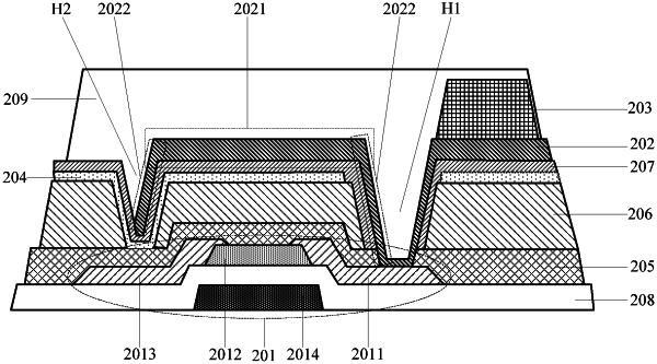
1. A detection substrate, comprising:
a base substrate;
a plurality of transistors on the base substrate;
a plurality of read electrodes on a side of each of the transistors away from the base substrate;
a plurality of photoelectric conversion structures on a side of each of the read electrodes away from the transistors;
an oxide layer on the side of each of the transistors away from the base substrate and on a side of each of the read electrodes facing the transistors; and
an insulating layer on the side of each of the transistors away from the base substrate and on the side of each of the read electrodes facing the transistors;
wherein the insulating layer comprises:
a first passivation layer on the side of each of the transistors away from the base substrate and on a side of the oxide layer facing the transistors;
a first resin layer on a side of the oxide layer away from the transistors and on the side of each of the read electrodes facing the transistors; and
a second passivation layer on a side of the first resin layer away from the oxide layer and on the side of each of the read electrodes facing the transistors;
wherein:
a first electrode of each of the transistors is electrically connected with each of the photoelectric conversion structures in a one-to-one correspondence mode via each of the read electrodes;
a material of an active layer of each of the transistors comprises an oxide;
each of the photoelectric conversion structures comprises: an N-type semiconductor layer, an intrinsic semiconductor layer, and a P-type semiconductor layer;
the oxide layer at least covers channel regions of the transistors and is insulated from the read electrodes;
the first resin layer has a first via in a region where a second electrode of the transistor is located, and the second passivation layer covers the first via, and the read electrode at least covers part of the first via; and
an orthographic projection of the oxide layer onto the base substrate covers an orthographic projection of the first via onto the base substrate.
|