| CPC H01L 27/14603 (2013.01) [A61B 1/00009 (2013.01); A61B 1/051 (2013.01); A61B 1/0676 (2013.01); H01L 24/17 (2013.01); H01L 24/20 (2013.01); H01L 24/28 (2013.01); H01L 25/0657 (2013.01); H01L 27/124 (2013.01); H01L 27/146 (2013.01); H01L 27/14601 (2013.01); H01L 27/14609 (2013.01); H01L 27/14618 (2013.01); H01L 27/14634 (2013.01); H01L 27/14636 (2013.01); H01L 27/14638 (2013.01); H01L 27/1464 (2013.01); H01L 27/14641 (2013.01); H01L 27/14643 (2013.01); H01L 27/14689 (2013.01); H01L 27/1469 (2013.01); H04N 23/56 (2023.01); H04N 25/75 (2023.01); H04N 25/767 (2023.01); H04N 25/772 (2023.01); H04N 25/778 (2023.01); H04N 25/79 (2023.01); H01L 31/028 (2013.01); H01L 31/0296 (2013.01); H01L 31/0304 (2013.01); H01L 2924/0002 (2013.01); H01L 2924/381 (2013.01); H04N 23/555 (2023.01)] | 20 Claims |

|
1. An imaging sensor comprising:
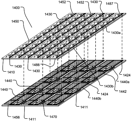
a pixel array comprising a plurality of pixels formed into a plurality of pixel columns, wherein the plurality of pixel columns are divided into a plurality of pixel sub-columns;
a plurality of pixel sub-column buses that correspond with the plurality of pixel sub-columns, such that at least one of the plurality of pixel sub-column buses is associated with one of the plurality of pixel sub-columns such that each of the plurality of pixel sub-columns are configured to be read independently;
a plurality of supporting circuits configured to process data received from the plurality of pixels, wherein the plurality of supporting circuits are formed into a plurality of supporting circuit columns, and wherein the plurality of supporting circuit columns are divided into a plurality of supporting circuit sub-columns;
a plurality of supporting circuit sub-column buses that correspond with the plurality of supporting circuit sub-columns, such that at least one of the plurality of supporting circuit sub-column buses is associated with one of the plurality of supporting circuit sub-columns;
wherein at least a portion of the plurality of supporting circuit sub-column buses and at least a portion of the plurality of pixel sub-columns buses are superimposed; and
a plurality of interconnects, wherein at least one interconnect electrically connects each of the plurality of pixel sub-column buses to each of the plurality of supporting circuit sub-column buses such that each of the plurality of supporting circuit sub-columns receives pixel data from a corresponding pixel sub-column;
wherein the plurality of interconnects are positioned anywhere along an intercept of the plurality of pixel sub-column buses and the plurality of circuit sub-column buses, wherein the intercept is defined by the superimposition of the at least a portion of the plurality of pixel sub-column buses directly with the at least a portion of the plurality of the circuit sub-column buses.
|