| CPC H01L 23/53238 (2013.01) [C25D 3/38 (2013.01); C25D 5/48 (2013.01); C25D 7/12 (2013.01); H01L 21/2885 (2013.01); H01L 21/7684 (2013.01); H01L 21/76877 (2013.01); H01L 23/53252 (2013.01)] | 19 Claims |

|
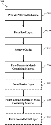
1. An electroplating method comprising:
plating a metal material into at least one opening on a patterned substrate, wherein at least a portion of the metal material is characterized by a nanotwin crystal structure; and
polishing an exposed surface of the metal material in the opening to reduce an average surface roughness of the exposed surface to less than or about 1 nm, wherein the polished exposed surface comprises at least a portion of the metal material characterized by the nanotwin crystal structure.
|