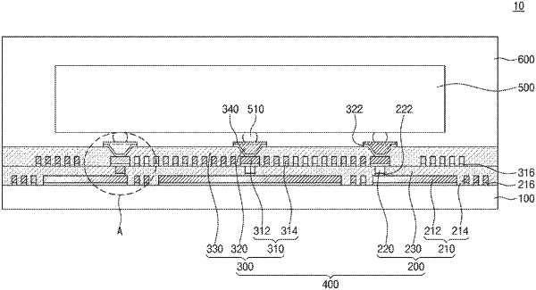
| CPC H01L 23/5226 (2013.01) [H01L 21/565 (2013.01); H01L 21/76819 (2013.01); H01L 21/76871 (2013.01); H01L 21/76877 (2013.01); H01L 23/3128 (2013.01); H01L 23/5283 (2013.01); H01L 24/09 (2013.01); H01L 24/17 (2013.01); H01L 2224/0231 (2013.01); H01L 2224/02373 (2013.01); H01L 2224/02381 (2013.01); H01L 2224/0401 (2013.01)] | 20 Claims |

|
1. A redistribution substrate comprising:
a first conductive pattern;
a first seed layer on a bottom surface of the first conductive pattern;
a first via connected to a top surface of the first conductive pattern, the top surface of the first conductive pattern and a lateral surface of the first via are substantially perpendicular;
a second seed layer between the first via and the first conductive pattern;
a first dielectric layer that encapsulates the first conductive pattern and the first via, a top surface of the first dielectric layer being coplanar with a top surface of the first via;
a second conductive pattern on the top surface of the first via;
a third seed layer on a bottom surface of the second conductive pattern;
a second via connected to a top surface of the second conductive pattern, the top surface of the second conductive pattern and a lateral surface of the second via are substantially perpendicular;
a fourth seed layer between the second via and the second conductive pattern; and
a second dielectric layer that encapsulates the second conductive pattern and the second via on the first dielectric layer.
|