| CPC H01L 23/481 (2013.01) [H01L 21/4814 (2013.01); H01L 25/18 (2013.01)] | 21 Claims |

|
1. A method comprising:
etching a through-substrate via (TSV) in a semiconductor substrate from a backside of the semiconductor substrate up to an insulator layer on a frontside of the semiconductor substrate, the insulator layer being exposed at a bottom of the TSV;
depositing an insulating liner on a sidewall of the TSV up to the insulator layer on the frontside of the semiconductor substrate and on the insulator layer exposed at the bottom of the TSV:
depositing a spacer layer, conformally, on the backside of the semiconductor substrate, and on the insulating liner deposited on the sidewall and the bottom of the TSV;
etching the spacer layer to form a self-aligned mask for etching a contact opening through the insulator layer at the bottom of the TSV to a metal pad inside the insulator layer, the self-aligned mask being formed by the spacer layer deposited on the sidewall of the TSV;
etching, through the self-aligned mask, the contact opening through the insulator layer at the bottom of TSV to the metal pad inside the insulator layer; and
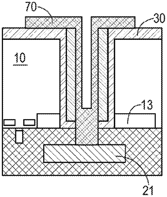
filling the contact opening through the insulator layer at the bottom of TSV with a conductive material, and depositing a layer of the conductive material on the sidewall of the TSV to form a vertical interconnection from the backside of the semiconductor substrate to the metal pad, the vertical interconnection having a step shape with a width of the vertical interconnection in the contact opening being smaller than the width of the vertical interconnection in the TSV.
|