| CPC H01L 22/20 (2013.01) [G06N 20/00 (2019.01); H01L 22/14 (2013.01)] | 12 Claims |

|
1. A method, comprising:
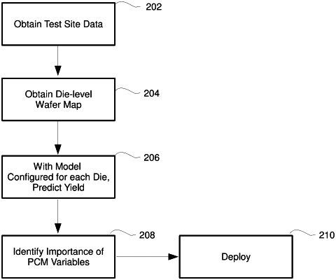
obtaining testing data from each of a respective plurality of test sites formed and distributed across a semiconductor wafer, prior to slicing a multiplicity of dies from the wafer;
obtaining a die level map of the semiconductor wafer that includes graphical details regarding a multiplicity of semiconductor features and corresponding locations for each feature on the semiconductor wafer; and
for each of the multiplicity of dies on the semiconductor wafer:
providing the testing data and the die level map as input data to a multiplicity of neural networks, each neural network corresponding to a respective one of the multiplicity of dies and each neural network programmed with instructions to (i) determine non-linear relationships among the input data for the respective die, (ii) impute from the determined non-linear relationship among the input data a plurality of input process parameters relevant to the respective die, and (iii) predict yield for the respective die from the imputed input process parameters, wherein each neural network is initially configured from training sets of input data.
|