US 11,972,952 B2
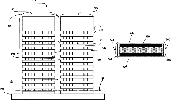
Atomic layer deposition on 3D NAND structures
Ruopeng Deng, San Jose, CA (US); Xiaolan Ba, Fremont, CA (US); Tianhua Yu, Tracy, CA (US); Yu Pan, San Jose, CA (US); and Juwen Gao, San Jose, CA (US)
Assigned to Lam Research Corporation, Fremont, CA (US)
Appl. No. 17/312,594
Filed by Lam Research Corporation, Fremont, CA (US)
PCT Filed Dec. 13, 2019, PCT No. PCT/US2019/066301
§ 371(c)(1), (2) Date Jun. 10, 2021,
PCT Pub. No. WO2020/123987, PCT Pub. Date Jun. 18, 2020.
Claims priority of provisional application 62/780,006, filed on Dec. 14, 2018.
Prior Publication US 2021/0335617 A1, Oct. 28, 2021
Int. Cl. H01L 21/76 (2006.01); H01L 21/285 (2006.01); H01L 21/768 (2006.01); H10B 41/27 (2023.01); H10B 43/27 (2023.01)
CPC H01L 21/28562 (2013.01) [H01L 21/28568 (2013.01); H01L 21/76876 (2013.01); H01L 21/76877 (2013.01); H10B 41/27 (2023.02); H10B 43/27 (2023.02)] 16 Claims
OG exemplary drawing
 
1. A method comprising:
providing a structure to be filled with a tungsten-containing material;
exposing the structure to multiple deposition cycles, wherein each deposition cycle comprises sequentially delivering a dose of hydrogen (H2) co-flowed with nitrogen (N2) and a dose of a tungsten precursor to a chamber housing the structure,
wherein the N2 is greater than 30% (vol) of the total N2+H2 flow and the substrate temperature is at least 375° C. during the dose of H2 co-flowed with N2.