| CPC H01J 37/32146 (2013.01) [H01J 37/321 (2013.01); H01J 37/32155 (2013.01); H01J 37/32568 (2013.01); H01L 21/31116 (2013.01); H01L 21/31144 (2013.01); H01L 21/67069 (2013.01); H01L 21/6831 (2013.01); H01J 2237/3343 (2013.01)] | 16 Claims |

|
1. A plasma processing apparatus comprising:
a plasma processing chamber;
a substrate support disposed in the plasma processing chamber and including a lower electrode;
a source RF generator coupled to the plasma processing chamber and configured to generate a source RF signal including high states and low states in alternate manner;
a bias DC generator coupled to the lower electrode and configured to generate a bias DC signal;
a non-transitory memory device that holds computer readable instructions therein; and
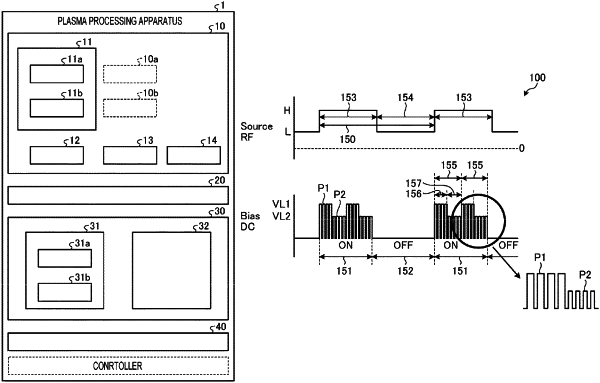
a controller having a processor that is configured by execution of the computer readable instructions to control an operation of the source RF generator and an operation of the bias DC generator, the operation of the bias DC generator being controlled by the controller to generate the DC bias signal to include ON states and OFF states in alternate manner, periods of the ON states of the bias DC signal corresponding to periods of the high states of the source RF signal, respectively, periods of the OFF states of the bias DC signal corresponding to periods of the low states of the source RF signal, respectively, each ON state of the bias DC signal including a plurality of cycles, each cycle including a first sequence of first pulses and a second sequence of second pulses, each first pulse having a first voltage level, and each second pulse having a second voltage level different from the first voltage level.
|