| CPC G09G 3/3258 (2013.01) [G09G 3/3291 (2013.01); G11C 19/28 (2013.01); G09G 2310/0286 (2013.01)] | 20 Claims |

|
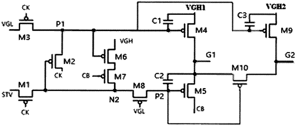
1. A shift register unit, configured to generate a first gate drive signal and a second gate drive signal, the shift register unit comprising:
a first control circuit, configured to control a potential of a first node, wherein the first control circuit comprises a first control transistor and a second control transistor,
a second control circuit, configured to control a potential of a second node, wherein the second control circuit comprises a third control transistor, a fourth control transistor, a fifth control transistor, and a sixth control transistor,
a first output circuit, configured to generate the first gate drive signal based on a first voltage signal provided by a first voltage terminal under the control of the potentials of the first and second nodes, and output the first gate drive signal through a first gate drive signal output terminal, wherein the first voltage signal provided by the first voltage terminal is a high level signal, and
a second output circuit, configured to generate a second gate drive signal based on a second voltage signal provided by a second voltage terminal under the control of a potential of a control node, and output the second gate drive signal through a second gate drive signal output terminal,
wherein the third control transistor comprises a control electrode electrically connected to a second clock signal terminal,
the first output circuit comprising:
a first output transistor, comprising a control electrode electrically connected to the first node, a first electrode electrically connected to the first voltage terminal, and a second electrode electrically connected to the first gate drive signal output terminal,
a first output pull-down transistor, comprising a control electrode electrically connected to the control node, a first electrode electrically connected to the first gate drive signal output terminal, and a second electrode electrically connected to a first clock signal terminal, and
an output pull-down capacitor, comprising a first terminal electrically connected to the second node, and a second terminal electrically connected to the first gate drive signal output terminal;
wherein the second output circuit further comprises a second output pull-down transistor having its gate electrode electrically connected to the control node;
wherein the first voltage terminal and the second voltage terminal are provided with substantially different potential values; and
wherein when (i) the second clock signal terminal is inputted with a low level, (ii) the first clock signal terminal is inputted with a high level, and (iii) a starting voltage is of a high level, then a potential of the first node is of a low level, potentials of a second control node and the second node are both of high levels, the third control transistor, the first control transistor, the first output transistor, the fourth control transistor, and the sixth control transistor are turned on, and the first gate drive signal output terminal is outputted with a high level, wherein the first clock signal and the second clock signal are pulse signals used for switching between the high level and the low level.
|