| CPC G09G 3/20 (2013.01) [G09G 2300/0439 (2013.01); G09G 2320/0233 (2013.01); G09G 2330/10 (2013.01)] | 20 Claims |

|
1. An electronic device comprising:
an electronic display comprising a plurality of display pixels configured to display an image comprising image content; and
image processing circuitry configured to:
receive image data corresponding to the image;
identify one or more angular features of the image content of the image;
select a compensation mask from a plurality of compensation masks based on the one or more angular features of the image content;
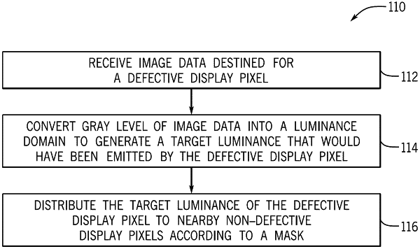
convert a gray level of the image data corresponding to a defective display pixel of the plurality of display pixels into a luminance domain to generate a target luminance that would have been emitted by the defective display pixel; and
distribute the target luminance of the defective display pixel to a nearby plurality of non-defective display pixels of the electronic display within a distance of the defective display pixel according to the selected compensation mask.
|