| CPC G02F 1/1368 (2013.01) [G02F 1/136254 (2021.01); G02F 1/136286 (2013.01)] | 11 Claims |

|
1. A display substrate, comprising:
a base substrate having a peripheral region; and
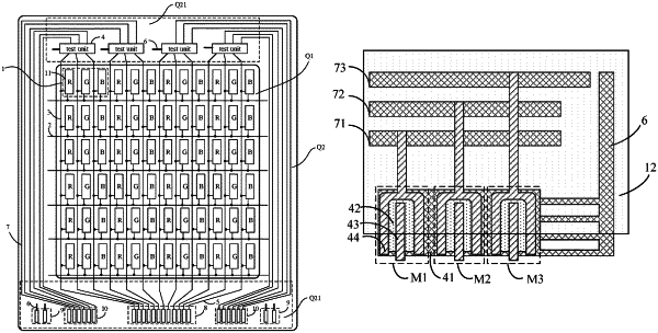
at least one test unit in the peripheral region of the base substrate, each of the at least one test unit comprising a plurality of thin film transistors,
wherein the plurality of thin film transistors share a gate electrode, and the shared gate electrode comprises a plurality of sub-electrodes arranged at intervals and each extending in a first direction,
the display substrate further comprises a switch signal line coupled to the test unit, and a different test unit is coupled to a different switch signal line, and
the switch signal line has a main body extending in a second direction that intersects the first direction and a plurality of tooth each extending in the first direction from the main body, the plurality of tooth are coupled to the sub-electrodes in one-to-one correspondence, and each tooth and the sub-electrode coupled thereto are an integral structure.
|