US 11,971,405 B2
Nanosensors and methods of making and using nanosensors
Georgios Alexandrakis, Arlington, TX (US); Jon Weidanz, Arlington, TX (US); Muhammad Usman Raza, Arlington, TX (US); and Sai Santosh Sasank Peri, Arlington, TX (US)
Assigned to BOARD OF REGENTS, THE UNIVERSITY TEXAS SYSTEM, Austin, TX (US)
Appl. No. 16/770,841
Filed by Board of Regents, The University of Texas System, Austin, TX (US)
PCT Filed Dec. 11, 2018, PCT No. PCT/US2018/064999
§ 371(c)(1), (2) Date Jun. 8, 2020,
PCT Pub. No. WO2019/118495, PCT Pub. Date Jun. 20, 2019.
Claims priority of provisional application 62/597,727, filed on Dec. 12, 2017.
Prior Publication US 2020/0393456 A1, Dec. 17, 2020
Int. Cl. G01N 33/543 (2006.01); B82Y 15/00 (2011.01); G01N 21/64 (2006.01); G01N 33/487 (2006.01)
CPC G01N 33/54373 (2013.01) [B82Y 15/00 (2013.01); G01N 21/648 (2013.01); G01N 33/487 (2013.01)] 20 Claims
OG exemplary drawing
 
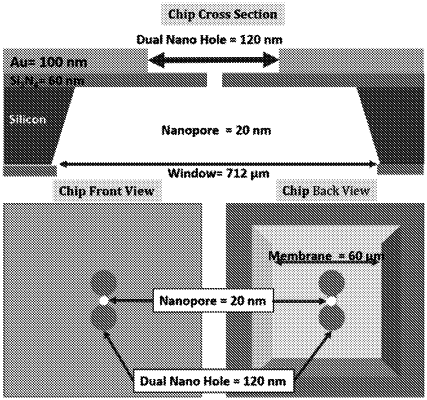
1. A sensor comprising:
a first layer having at least one dual nanohole structure, and
a second layer having at least one nanopore,
wherein the dual nanohole structure comprises a first nanohole and a second nanohole connected by a gap;
wherein the gap of the first layer is aligned with the nanopore of the second layer in a direction corresponding to a translocation direction across the first and second layers;
wherein the gap has a width of 10-50 nm; and
wherein the at least one nanopore entirely passes through the second layer in the translocation direction.