| CPC H01L 29/404 (2013.01) [H01L 29/778 (2013.01); H01L 29/872 (2013.01)] | 13 Claims |
|
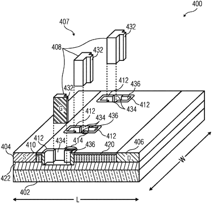
1. A field-effect transistor (FET), comprising:
a substrate;
source and drain electrodes on the substrate;
a channel layer;
a gate electrode structure comprising:
a gate electrode in contact with the channel layer; and
a first lateral field plate adjacent to the gate electrode; and
a first dielectric layer disposed between the first lateral field plate and the channel layer;
wherein the first lateral field plate is in contact with the first dielectric layer and is configured to modulate an electric field proximal to the gate electrode proximal to at least one of or both the drain or source electrodes, and
wherein the gate electrode and the first lateral field plate comprise top and bottom portions,
wherein the bottom portions of the gate electrode and the first lateral field plate are buried in an aperture defined in the substrate to a depth extending to the channel layer and the top portions of the gate electrode and the first lateral field plate extend above a surface of the substrate.
|