| CPC G11C 16/0483 (2013.01) [H01L 23/5226 (2013.01); H01L 23/5283 (2013.01); H10B 41/10 (2023.02); H10B 41/27 (2023.02); H10B 41/35 (2023.02); H10B 43/10 (2023.02); H10B 43/27 (2023.02); H10B 43/35 (2023.02)] | 23 Claims |

|
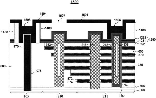
1. A method for forming a three-dimensional (3D) memory device, comprising:
disposing an alternating dielectric stack over a substrate, wherein the alternating dielectric stack includes first dielectric layers and second dielectric layers alternatingly stacked on the substrate;
forming a channel structure penetrating through the alternating dielectric stack and extending into the substrate, wherein the channel structure includes a channel layer disposed on a sidewall of a memory film;
removing the substrate and a portion of the memory film that extends into the substrate to expose a portion of the channel layer;
disposing an array common source (ACS) on the exposed portion of the channel layer;
disposing an ACS contact structure to contact the ACS; and
disposing a through-silicon-via (TSV) contact structure to contact a TSV. wherein an isolation spacer formed on a sidewall of the TSV contact structure extends through the ACS and isolates the TSV and the ACS.
|