| CPC H10K 50/8426 (2023.02) [H10K 71/00 (2023.02); H10K 59/131 (2023.02); H10K 59/40 (2023.02)] | 12 Claims |
|
1. A display device, comprising:
a display panel comprising a display region and a non-display region;
a window member on the display panel; and
an adhesive member between the display panel and the window member, the adhesive member comprising:
a first adhesion portion overlapping with the display region in a plan view; and
a second adhesion portion extending from the first adhesion portion and overlapping with the non-display region in the plan view,
wherein the display panel comprises:
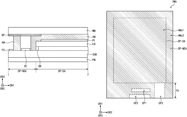
a substrate;
a display element layer on the substrate and overlapping with the display region;
a driving chip on the substrate and overlapping with the non-display region, the driving chip being configured to provide a driving signal to the display element layer;
a pad region comprising pads on the substrate, the pads being electrically connected to the driving chip, the driving chip being, when viewed in the plan view, between the display region and the pad region; and
an encapsulation member on the display element layer,
wherein, in the plan view, the window member overlaps with the driving chip and the second adhesion portion,
wherein the first adhesion portion connects the window member to the encapsulation member,
wherein the second adhesion portion is integrally formed with the first adhesion portion and attaches the window member to the substrate,
wherein the second adhesion portion encloses the driving chip,
wherein the second adhesion portion comprises:
a first opening overlapping with the driving chip in the plan view; and
a second opening exposing the pad region, the second opening being, when viewed in the plan view, spaced apart from the first opening; and
a third opening exposing an input sensing circuit,
wherein, when viewed in the plan view, the second adhesion portion is spaced apart from the driving chip and the pads,
wherein the first opening is parallel to the second opening when viewed in the plan view,
wherein the first opening and the second opening are provided in the second adhesion portion and not in the first adhesion portion,
wherein the third opening is perpendicular to the first and second openings when viewed in the plan view, in which the third opening extends across an entire width of the second adhesion portion to an edge of the first adhesion portion.
|