| CPC H10B 43/35 (2023.02) [G11C 16/0466 (2013.01); G11C 16/0483 (2013.01); H10B 43/27 (2023.02); H10B 43/40 (2023.02); G11C 16/10 (2013.01); G11C 16/26 (2013.01)] | 6 Claims |
|
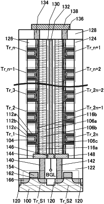
1. A semiconductor device comprising:
a substrate;
a first insulator;
a first conductor over the first insulator;
a second conductor over the first insulator;
an oxide semiconductor over and in contact with the first conductor and the second conductor;
a first gate insulator including a region facing a side of the oxide semiconductor;
a first gate electrode including a region facing the side of the oxide semiconductor with the first gate insulator therebetween;
a second gate insulator including a region facing the side of the oxide semiconductor;
a second gate electrode including a region facing the side of the oxide semiconductor with the second gate insulator therebetween;
a third conductor over and in contact with the oxide semiconductor;
a fourth conductor over and in contact with the oxide semiconductor; and
a fifth conductor over and in contact with the third conductor and the fourth conductor,
wherein the second gate electrode is over the first gate electrode.
|