| CPC H10B 43/27 (2023.02) [H01L 29/40114 (2019.08); H01L 29/40117 (2019.08); H10B 41/10 (2023.02); H10B 41/27 (2023.02); H10B 41/50 (2023.02); H10B 43/10 (2023.02); H10B 43/50 (2023.02)] | 14 Claims |
|
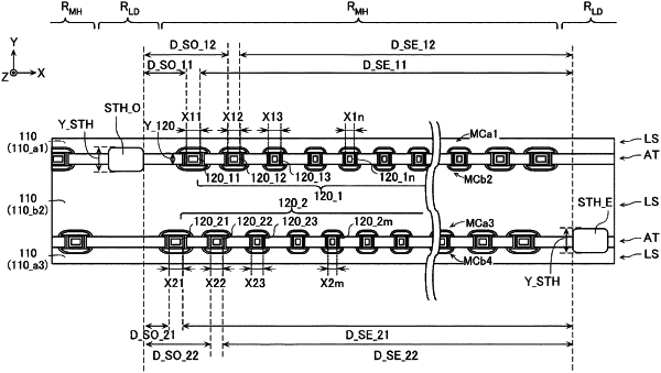
1. A semiconductor storage device comprising:
a first conductive layer extending in a first direction;
a second conductive layer extending in the first direction and disposed apart from the first conductive layer in a second direction intersecting the first direction;
a third conductive layer extending in the first direction and disposed apart from the first conductive layer and the second conductive layer in the second direction;
a plurality of first semiconductor layers interposed between the first conductive layer and the second conductive layer, each of the plurality of first semiconductor layers including regions adjacent the first conductive layer and the second conductive layer, respectively;
a plurality of first memory cells interposed between the first conductive layer and the plurality of first semiconductor layers;
a plurality of second memory cells interposed between the second conductive layer and the plurality of first semiconductor layers;
a plurality of second semiconductor layers interposed between the second conductive layer and the third conductive layer, each of the plurality of second semiconductor layers including regions adjacent the second conductive layer and the third conductive layer, respectively;
a plurality of third memory cells interposed between the second conductive layer and the plurality of second semiconductor layers;
a plurality of fourth memory cells interposed between the third conductive layer and the plurality of second semiconductor layers;
a first insulating layer interposed between the first conductive layer and the second conductive layer, the first insulating layer being wider than the plurality of first semiconductor layers and the plurality of second semiconductor layers in the second direction; and
a second insulating layer interposed between the second conductive layer and the third conductive layer, the second insulating layer being wider than the first semiconductor layers and the second semiconductor layers in the second direction,
wherein a third semiconductor layer and a fourth semiconductor layer from among the plurality of first semiconductor layers are provided as follows: the third semiconductor layer has a first width in the first direction; the third semiconductor layer and the first insulating layer are disposed apart from each other in the first direction with a first distance; the third semiconductor layer and the second insulating layer are disposed apart from each other in the first direction with a second distance; the fourth semiconductor layer has a second width in the first direction; the fourth semiconductor layer and the first insulating layer are disposed apart from each other in the first direction with a third distance; and the fourth semiconductor layer and the second insulating layer are disposed apart from each other in the first direction with a fourth distance,
wherein a shorter one of the first distance and the second distance is shorter than a shorter one of the third distance and the fourth distance, and the first width is larger than the second width.
|