| CPC H10B 12/053 (2023.02) [H01L 21/30604 (2013.01); H01L 21/3081 (2013.01); H01L 21/3086 (2013.01); H01L 21/76224 (2013.01); H10B 12/34 (2023.02)] | 20 Claims |
|
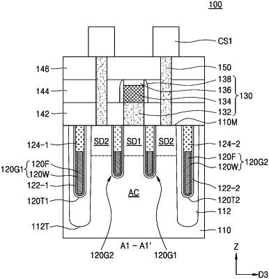
1. An integrated circuit device comprising:
a substrate comprising a memory cell area;
a plurality of first gate electrodes in a plurality of first trenches in the memory cell area of the substrate and extending in a first direction parallel to a top surface of the substrate;
a plurality of second gate electrodes in a plurality of second trenches in the memory cell area of the substrate, the second gate electrodes extending in the first direction,
wherein the plurality of first gate electrodes alternate with the plurality of second gate electrodes in a second direction, the second direction parallel to the top surface of the substrate and perpendicular to the first direction,
a first end portion of each of the plurality of first gate electrodes is spaced apart from an edge of the memory cell area by a first distance, and
a second end portion of each of the plurality of second gate electrodes is spaced apart from the edge of the memory cell area by a second distance different from the first distance; and
device isolation layers in the substrate, the device isolation layers defining a plurality of active layers,
wherein the plurality of first trenches comprise first portions vertically overlapping a plurality of active areas and second portions vertically overlapping the device isolation layers,
bottom surfaces of the first portions have a first depth from the top surface of the substrate, bottom surfaces of the second portions have a second depth greater than the first depth from the top surface of the substrate,
the plurality of second trenches comprise third portions vertically overlapping the plurality of active areas and fourth portions vertically overlapping the device isolation latyers,
bottom surfaces of the third portions have a third depth from the top surface of the substrate, and
bottom surfaces of the fourth portions have a fourth depth greater than the third depth from the top surface of the substrate.
|