| CPC H10B 12/00 (2023.02) [G11C 11/405 (2013.01); G11C 11/4074 (2013.01); H01L 29/66083 (2013.01)] | 10 Claims |
|
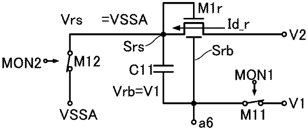
1. A method for operating a semiconductor device comprising a first transistor, a first capacitor, a first output terminal, a first switch, and a second switch,
wherein a gate and a source of the first transistor are electrically connected to each other,
wherein a first terminal of the first capacitor and the first output terminal are electrically connected to a back gate of the first transistor,
wherein a second terminal of the first capacitor is electrically connected to the source,
wherein the first switch controls input of a first voltage to the back gate,
wherein a second voltage is input to a drain of the first transistor, and
wherein the second switch controls input of a third voltage to the source,
the method comprising:
turning on the first switch and the second switch in a first period;
turning off the second switch in a second period after the first period;
turning off the first switch in a third period after the second period; and
turning on the second switch in a fourth period after the third period.
|