| CPC H05K 3/467 (2013.01) [H05K 1/0271 (2013.01); H05K 1/181 (2013.01); H05K 1/183 (2013.01); H05K 1/185 (2013.01); H05K 3/4697 (2013.01)] | 20 Claims |
|
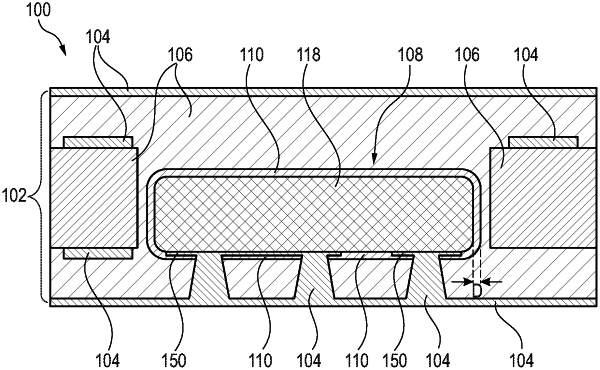
1. A method of manufacturing a component carrier, comprising:
providing a laminated stack having at least one electrically conductive layer structure and/or at least one electrically insulating layer structure;
at least partially covering a component with a transition layer having a thickness in a range from 1.0 nm to 100 nm;
assembling the component with the stack; and
at least partially covering a redistribution layer by the transition layer;
wherein the component carrier is a printed circuit board or IC substrate, and
wherein surfaces of the component except for at least one portion of at least one component pad being directly electrically connected to the at least one electrically conductive layer structure, are in direct contact with the transition layer.
|