| CPC H05K 1/111 (2013.01) [H05K 3/22 (2013.01); H05K 3/4644 (2013.01); H05K 2201/10227 (2013.01)] | 8 Claims |
|
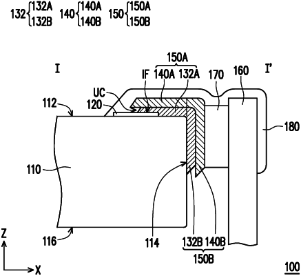
1. A panel device, comprising:
a substrate, having a first surface and a second surface connected to the first surface, wherein a normal direction of the second surface is different from a normal direction of the first surface;
a conductor pad, disposed on the first surface of the substrate;
a turning wire, disposed on the substrate and extending from the first surface to the second surface, wherein the turning wire comprises a wiring layer in contact with the conductor pad and a wire covering layer covering the wiring layer; and
a circuit board, bonded to the wire covering layer and electrically connected to the wire covering layer,
wherein an area of the projection of the wire covering layer on the first surface is greater than an area of the projection of the wiring layer on the first surface.
|