| CPC H04N 25/77 (2023.01) [H01L 27/14612 (2013.01); H04N 25/573 (2023.01); H04N 25/766 (2023.01)] | 22 Claims |
|
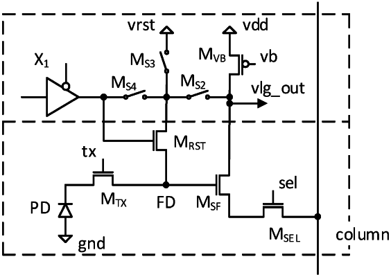
1. An image sensor comprising a plurality of pixel circuits each comprising:
a photodiode connected between ground and a floating diffusion (FD) node,
a reset transistor (MRST) configured to be connected between a first voltage supply and the floating diffusion (FD) node,
a source follower transistor (MSF), wherein a drain of the source follower transistor (MSF) is connected to a second voltage supply, a gate of the source follower transistor (MSF) is connected to the floating diffusion (FD) node and a source of the source follower transistor (MSF) is connected to a row select transistor (MSEL), and
the row select transistor (MSEL) is connected between the source of the source follower transistor (MSF) and a common column output,
wherein each pixel circuit is configured to provide an output signal corresponding to a light incident on the photodiode; and
wherein, to configure each pixel circuit to selectively output a linear integration signal or a logarithmic signal, each pixel circuit further comprises:
a first additional bias transistor (MVB) connected between the second voltage supply and the drain of the source follower transistor (MSF), and
a second additional transistor (MS2) configured to connect a drain of the bias transistor (MVB) to a drain of the reset transistor (MRST), and
a third additional transistor (MS3) configured to connect the reset transistor (MRST) to the first voltage supply, and
a fourth additional transistor (MS4) configured to connect the drain of the reset transistor (MRST) to a gate of the reset transistor (MRST).
|