| CPC H04N 25/46 (2023.01) [H04N 25/70 (2023.01)] | 20 Claims |
|
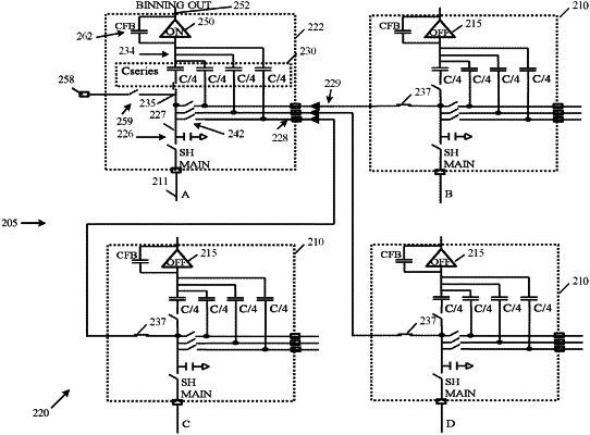
1. An apparatus comprising:
analog pixel processing circuitry configured to process an analog pixel signal of a pixel, the analog pixel processing circuitry comprising:
a first input to input the analog pixel signal of the pixel;
Sample and Hold (SH) circuitry configured to provide an analog sample of the pixel based on the analog pixel signal;
one or more second inputs to input analog samples of one or more binning pixels, respectively;
a plurality of capacitors having capacitor output terminals connected to a common output terminal, wherein a capacitor input terminal of a first capacitor of the plurality of capacitors is connected to an input terminal to input the analog sample of the pixel from the SH circuitry, wherein capacitor input terminals of one or more second capacitors of the plurality of capacitors are connected to the one or more second inputs, respectively;
a switchable connector switchable between a first state and a second state, wherein at the first state the switchable connector is to connect the capacitor input terminals of the one or more second capacitors to the input terminal such that the plurality of capacitors are to be connected in parallel between the input terminal and the common output terminal, wherein at the second state the switchable connector is to disconnect the capacitor input terminals of the one or more second capacitors from the input terminal; and
an amplifier configured to provide an amplified analog signal by amplifying an analog signal from the common output terminal.
|