| CPC H04L 9/3278 (2013.01) [G06F 21/44 (2013.01); H04L 2209/12 (2013.01)] | 16 Claims |
|
1. A semiconductor device including circuitry configured to derive a physical unclonable function, the circuitry comprising:
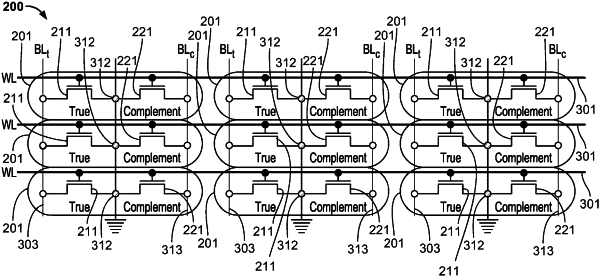
a plurality of bitcells, wherein: each bitcell in the plurality of bitcells comprises a differential transistor pair including a plurality, fewer than three, of transistors,
each bitcell outputs a ‘1’ value when a threshold voltage of a first transistor in the plurality of transistors exceeds a threshold voltage of a second transistor in the plurality of transistors, and
each bitcell outputs a ‘0’ value when the threshold voltage of the second transistor exceeds the threshold voltage of the first transistor; and
sense amplifier circuitry configurable to read values from the plurality of bitcells, the sense amplifier circuitry comprising:
differential sense amplifier circuitry having a current stage and a voltage stage, the current stage having a first leg coupled to a bit line of the first transistor and a second leg coupled to a bit line of the second transistor, the voltage stage comprising a comparator coupled between the first leg and the second leg, and
margin circuitry configurable (i) to selectably bias reading of the plurality of bitcells toward one of ‘0’ values and ‘1’ values by a current generator coupled to a respective one of the first leg and the second leg, and configured to selectably inject at any one time a margining current into at most one of the first leg and the second leg, (ii) to identify addresses of bitcells having a stable ‘1’ value when the margin circuitry is configured to bias reading of the plurality of bitcells toward ‘0’ values, and (iii) to identify addresses of bitcells having a stable ‘0’ value when the margin circuitry is configured to bias reading of the plurality of bitcells toward ‘1’ values.
|