| CPC H03K 3/037 (2013.01) [G01D 5/145 (2013.01); H03F 3/04 (2013.01); H03K 5/24 (2013.01)] | 7 Claims |
|
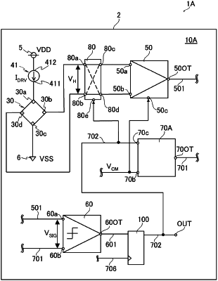
1. A semiconductor device comprising a magnetic switch provided on a semiconductor substrate, the magnetic switch comprising:
a Hall element comprising at least four electrodes;
a switch circuit which comprises an input terminal pair supplied with a differential output voltage from two electrodes among the four electrodes, an output terminal pair, and a control terminal, and is capable of switching a connection state between the input terminal pair and the output terminal pair between a first state and a second state based on a control signal supplied to the control terminal of the switch circuit;
an amplifier which amplifies a difference between signals supplied from the output terminal pair of the switch circuit;
a reference voltage circuit which generates a reference voltage based on a reference common mode voltage and the control signal which are received;
a comparator which compares an output signal of the amplifier with the reference voltage outputted from the reference voltage circuit; and
a latch circuit which latches an output voltage of the comparator and outputs the control signal, and which performs control to switch the reference voltage of the reference voltage circuit to one of a voltage obtained by applying an adjustment value to a reference value in a positive direction and a voltage obtained by applying the adjustment value to the reference value in a negative direction, according to the control signal corresponding to an output signal of the comparator.
|