| CPC H02M 3/1582 (2013.01) [H02M 1/0058 (2021.05); H02M 7/5387 (2013.01)] | 15 Claims |
|
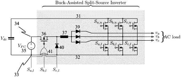
1. A buck-assisted split-source inverter comprising:
a DC link having two voltage rails;
at least two pairs of series connected switches with antiparallel diodes connected between the voltage rails of the DC link, center points of the series connected switches forming phase outputs of the inverter;
a first connection point and a second connection point for receiving voltage terminals of a fuel cell, one of the two voltage rails forming the first connection point;
a switch component and an inductor connected in series having a first end formed of a terminal of the switch component and a second end formed of a terminal of the inductor, the first end forming the second connection point for receiving a voltage terminal of the fuel cell;
at least two first diodes having one of their corresponding terminals connected together and to the second end of the series connection of the switch component and the inductor, and the other terminals of the at least two first diodes being connected to separate phase outputs of the inverter; and
a second diode having first and second terminals, the first terminal being connected to a point between the switch component and the inductor and the second terminal being connected to the voltage rail forming the first connection point, a polarity of the second diode corresponding to polarities of the at least two first diodes such that a current path is formed through the second diode and the at least two first diodes,
wherein the switch component is adapted to be controlled conductive when any one of the lower switches connected to the voltage rail forming the first connection point is controlled conductive.
|