| CPC H01P 5/16 (2013.01) [H05K 5/03 (2013.01); H05K 7/14 (2013.01)] | 16 Claims |

|
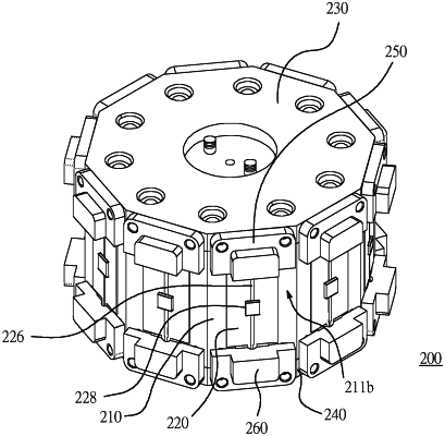
1. A power dividing and combining device, comprising:
a resonance body, comprising:
a solid conductive body, having a first surface, a second surface opposite to the first surface, and a plurality of side surfaces connecting the first surface and the second surface;
a plurality of first dividing elements, disposed on the first surface and separate a plurality of first resonance channels on the first surface, wherein the first resonance channels intersect at a first common region on the first surface;
a plurality of second dividing elements, disposed on the second surface and separate a plurality of second resonance channels on the second surface, wherein the second resonance channels intersect at a second common region on the second surface;
a signal-receiving end, disposed on the first surface and in the first common region; and
a signal-transmitting end, disposed on the second surface and in the second common region;
a plurality of circuit boards, disposed respectively on the side surfaces, wherein two opposite ends of each of the circuit boards respectively close one of the first resonance channels and one of the second resonance channels, and each of the circuit boards comprises a power-amplifying element;
an upper cover, disposed on the first dividing elements, wherein the first resonance channels are located in a first accommodating space formed by the upper cover, the circuit boards and the first surface of the solid conductive body; and
a lower cover, disposed on the second dividing elements, wherein the second resonance channels are located in a second accommodating space formed by the lower cover, the circuit boards and the second surface of the solid conductive body.
|