| CPC H01L 33/32 (2013.01) [H01L 27/153 (2013.01); H01L 27/156 (2013.01); H01L 33/0025 (2013.01); H01L 33/0075 (2013.01); H01L 33/06 (2013.01); H01L 33/24 (2013.01); H01L 33/38 (2013.01); H01L 33/502 (2013.01); H05B 45/30 (2020.01); H01L 2933/0016 (2013.01)] | 20 Claims |
|
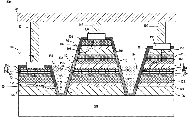
1. A light emitting diode (LED) array comprising:
a first mesa comprising a first top surface, at least a first LED including a first p-type layer, a first n-type layer, and a first color active region, and a first tunnel junction on the first LED, the top surface of the first mesa comprising a second n-type layer on the first tunnel junction, the second n-type layer comprising at least one n-type III-nitride layer with >10% Al mole fraction and at least one n-type III-nitride layer with <10% Al mole fraction;
an adjacent mesa comprising a top surface, the first LED, a second LED including the second n-type layer, a second p-type layer, and a second color active region;
a second tunnel junction on the second LED of the adjacent mesa, and a third n-type layer on the second tunnel junction of the adjacent mesa;
a first trench separating the first mesa and the adjacent mesa;
cathode metallization in the first trench extending continuously from the first color active region of the first mesa to the second color active region of the adjacent mesa; and
anode metallization contacts on the second n-type layer of the first mesa and on the top surface of the adjacent mesa.
|