| CPC H01L 31/022441 (2013.01) [H01L 29/456 (2013.01); H01L 31/1868 (2013.01)] | 8 Claims |

|
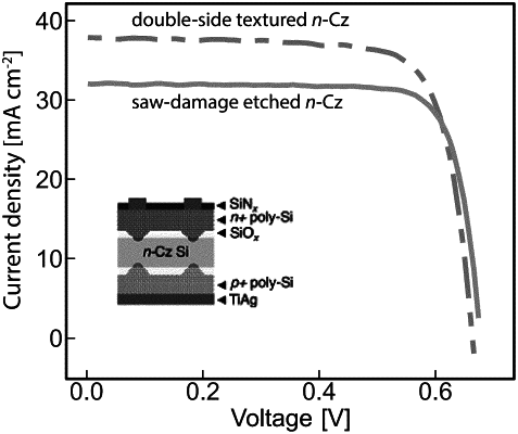
1. A double-side device comprising, in order:
a first silicon layer comprising n-doped polycrystalline silicon;
a first silicon oxide layer having a first thickness;
a second silicon layer comprising n-type crystalline silicon and having a first textured surface and a second textured surface;
a second silicon oxide layer having a second thickness; and
a third silicon layer comprising p-doped polycrystalline silicon, wherein:
a first plurality of conductive pathways comprising the n-doped polycrystalline silicon pass through the first thickness,
a second plurality of conductive pathways comprising the p-doped polycrystalline silicon pass through the second thickness,
the n-doped polycrystalline silicon penetrates into the second silicon layer forming a first plurality of penetrating regions within the second silicon layer, and
the p-doped polycrystalline silicon penetrates into the second silicon layer forming a second plurality of penetrating regions within the second silicon layer.
|