| CPC H01L 29/7869 (2013.01) [H01L 29/41733 (2013.01); H01L 29/41775 (2013.01); H01L 29/42384 (2013.01); H01L 29/78696 (2013.01); H10B 12/31 (2023.02)] | 15 Claims |
|
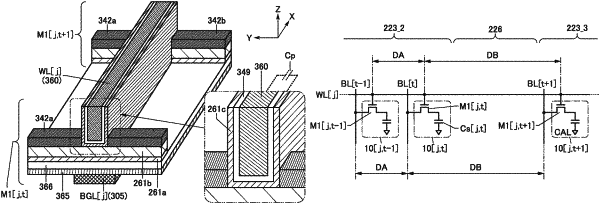
1. A memory device comprising:
a plurality of first wirings extending in a first direction;
a plurality of oxide layers; and
a first memory element group and a second memory element group,
wherein the plurality of first wirings comprise a region overlapping with the first memory element group, and a region overlapping with the second memory element group,
wherein one of the plurality of oxide layers comprises a region extending along a side surface of one of the first wirings,
wherein the first memory element group and the second memory element group comprise a plurality of memory elements,
wherein each of the plurality of memory elements comprises a transistor and a capacitor,
wherein in each of the plurality of memory elements, a gate electrode of the transistor is electrically connected to one of the plurality of first wirings, and a semiconductor layer of the transistor comprises a region in contact with one of the plurality of oxide layers, and
wherein a shortest distance from the gate electrode of the transistor included in the memory cell positioned in an end portion of the first memory element group to the gate electrode of the transistor included in the memory cell positioned in an end portion of the second memory element group is less than or equal to 3.5 μm.
|