| CPC H01L 28/92 (2013.01) [H01L 21/76877 (2013.01); H01L 21/76898 (2013.01); H01L 23/481 (2013.01); H01L 23/5223 (2013.01)] | 10 Claims |
|
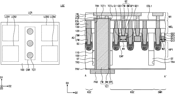
1. A semiconductor device comprising:
a semiconductor substrate including a connection region;
a pair of first epitaxial patterns provided at the semiconductor substrate;
a capacitor disposed between the pair of first epitaxial patterns;
a middle connection layer on the capacitor;
an interconnection layer on the middle connection layer; and
a through-via provided under the interconnection layer and penetrating the connection region of the semiconductor substrate,
wherein the capacitor comprises:
an upper portion of the semiconductor substrate between the pair of first epitaxial patterns;
a metal electrode on the upper portion of the semiconductor substrate; and
a dielectric pattern disposed between the upper portion of the semiconductor substrate and the metal electrode, and
wherein the through-via is connected to the capacitor through the interconnection layer and the middle connection layer, and
wherein the capacitor is adjacent to a sidewall of the through-via.
|