| CPC H01L 27/14636 (2013.01) [H01L 23/49811 (2013.01); H01L 23/49827 (2013.01); H01L 23/5286 (2013.01); H01L 24/19 (2013.01); H01L 24/20 (2013.01); H01L 27/14618 (2013.01); H01L 27/14678 (2013.01); G06V 40/12 (2022.01); H01L 21/568 (2013.01); H01L 2224/04105 (2013.01); H01L 2224/211 (2013.01); H01L 2224/214 (2013.01); H01L 2924/12042 (2013.01); H01L 2924/181 (2013.01); H01L 2924/18162 (2013.01)] | 20 Claims |
|
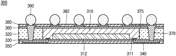
1. An electronic device comprising:
a semiconductor die comprising a first die side, a second die side opposite the first die side, and a plurality of lateral die sides extending between the first and second die sides, where the first die side comprises an integrated circuit and a bond pad;
an encapsulant that laterally covers the lateral die sides, where the encapsulant comprises a first encapsulant side, a second encapsulant side, and a plurality of lateral encapsulant sides extending between the first and second encapsulant sides;
a vertical interconnect structure passing through the encapsulant, the vertical interconnect structure comprising a first end and a second end;
a first conductor extending over the first die side and over the first encapsulant side, where the first conductor is coupled to the bond pad and to the first end of the vertical interconnect structure;
a second conductor coupled to the second end of the vertical interconnect structure;
a protection structure over the first die side and spaced apart from the first die side, wherein the protection structure forms a first exterior side of the electronic device with no conductive material exposed at the first exterior side;
a first dielectric material between the protection structure and the first die side, the first dielectric material configured to expose an area of the integrated circuit that is free of bond pads;
a second dielectric material on the second encapsulant side and laterally surrounding the second conductor, the second dielectric material forming a second exterior side of the electronic device, opposite the first exterior side; and
an external interconnect coupled to the second end of the vertical interconnect structure by the second conductor, wherein the external interconnect extends beyond the second exterior side formed by the second dielectric layer.
|