| CPC H01L 27/0886 (2013.01) [H01L 21/76232 (2013.01); H01L 21/823431 (2013.01); H01L 21/823481 (2013.01); H01L 21/823821 (2013.01); H01L 21/823878 (2013.01); H01L 27/0924 (2013.01); H01L 29/0653 (2013.01); H01L 29/66545 (2013.01); H01L 29/6656 (2013.01); H01L 29/66795 (2013.01); H01L 29/66818 (2013.01); H01L 29/7843 (2013.01); H01L 29/7846 (2013.01); H01L 29/7848 (2013.01); H01L 29/7851 (2013.01)] | 20 Claims |
|
1. An integrated circuit structure, comprising:
a nanowire along a direction;
a first isolation structure over a first end of the nanowire, wherein the first isolation structure has a top surface above the top of the nanowire;
a gate structure comprising a gate electrode completely surrounding a channel region of the nanowire, wherein the gate structure is spaced apart from the first isolation structure along the direction; and
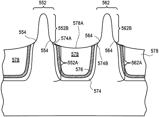
a second isolation structure over a second end of the nanowire, the second end opposite the first end, the second isolation structure spaced apart from the gate structure along the direction, wherein the second isolation structure has a top surface above the top of the nanowire, and wherein the first isolation structure and the second isolation structure each comprise a first dielectric material laterally surrounding a second dielectric material distinct from the first dielectric material, the second dielectric material having an upper surface, and wherein the wherein the first isolation structure and the second isolation structure both further comprise a third dielectric material laterally surrounded by an upper portion of the first dielectric material, the third dielectric material on the upper surface of the second dielectric material, and the third dielectric material distinct from the first dielectric material and from the second dielectric material.
|