| CPC H01L 25/18 (2013.01) [H01L 21/56 (2013.01); H01L 23/3107 (2013.01); H01L 23/49811 (2013.01); H01L 23/5383 (2013.01); H01L 23/5384 (2013.01); H01L 23/5386 (2013.01); H01L 24/48 (2013.01); H01L 25/50 (2013.01); H01L 2224/48141 (2013.01); H01L 2224/48227 (2013.01)] | 20 Claims |
|
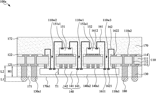
1. An electronic package, comprising:
a carrier having a first face and a second face opposite to the first face;
a first electronic component adjacent to the first face of the carrier;
an electrical extension structure adjacent to the first face of the carrier and defining a space with the carrier for accommodating the first electronic component, wherein the electrical extension structure is configured to connect the carrier with an external electronic component; and
an encapsulant encapsulating the first electronic component and at least a portion of the electrical extension structure,
wherein the carrier comprises a first opening connecting the first face and the second face, and a first type bonding wire passes through the first opening and connects to the first electronic component.
|