| CPC H01L 23/562 (2013.01) [H01L 23/49811 (2013.01); H01L 23/5386 (2013.01); H01L 24/14 (2013.01)] | 8 Claims |
|
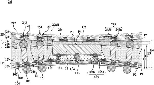
1. An electronic package structure, comprising:
an electronic structure;
a wiring structure disposed over the electronic structure;
a bonding element connecting the wiring structure and the electronic structure; and
a reinforcement element attached to the wiring structure;
wherein an elevation difference between a highest point and a lowest point of a surface of the wiring structure facing the electronic structure is less than a height of the bonding element,
wherein the bonding element and the reinforcement layer are disposed adjacent to two opposite sides of the wiring structure, respectively, and
wherein a hardness of the reinforcement element is greater than a hardness of the wiring structure.
|