| CPC H01L 23/5226 (2013.01) [H01L 21/76802 (2013.01); H01L 21/76877 (2013.01); H01L 23/562 (2013.01)] | 18 Claims |
|
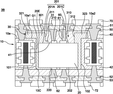
1. A semiconductor substrate structure, comprising:
a substrate defining a cavity;
an electronic device disposed in the cavity;
a filling material disposed on a first region of an upper surface of the electronic device;
a dielectric layer disposed over the electronic device and comprising an extending portion extending into the filling material; and
a first via in the dielectric layer, wherein the first via is horizontally overlapping and spaced apart from the filling material.
|