| CPC H01L 23/49894 (2013.01) [H01L 23/3121 (2013.01); H01L 23/42 (2013.01); H01L 23/433 (2013.01); H01L 23/49811 (2013.01); H01L 23/49816 (2013.01); H01L 23/49827 (2013.01); H01L 23/49833 (2013.01); H01L 25/105 (2013.01); H01L 23/5389 (2013.01); H01L 2224/16227 (2013.01); H01L 2224/32225 (2013.01); H01L 2224/48091 (2013.01); H01L 2224/48227 (2013.01); H01L 2224/73204 (2013.01); H01L 2224/73253 (2013.01); H01L 2224/73265 (2013.01); H01L 2224/92225 (2013.01); H01L 2225/1023 (2013.01); H01L 2225/1041 (2013.01); H01L 2225/1058 (2013.01); H01L 2225/107 (2013.01); H01L 2924/00014 (2013.01); H01L 2924/15311 (2013.01); H01L 2924/1533 (2013.01); H01L 2924/18161 (2013.01); H01L 2924/3511 (2013.01)] | 19 Claims |
|
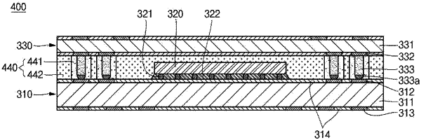
1. A semiconductor package comprising:
a substrate comprising a top substrate side, a bottom substrate side, a plurality of lateral substrate sides between the top and bottom substrate sides, and a top substrate circuit pattern on the top substrate side;
a semiconductor die mounted on the top substrate side, the semiconductor die comprising a top die side, a bottom die side facing the top substrate side, and a plurality of lateral die sides;
an interposer comprising:
a top interposer side;
a bottom interposer side;
a plurality of lateral interposer sides; and
a bottom interposer circuit pattern on the bottom interposer side;
a top adhesive that covers the top die side and bonds the top die side to the bottom interposer side;
a vertical interconnect structure comprising:
a top vertical interconnect end that is bonded to the bottom interposer circuit pattern; and
a bottom vertical interconnect end that is bonded to the top substrate circuit pattern; and
an encapsulating material, of a different material from the top adhesive, comprising a top encapsulant side facing the bottom interposer side, a bottom encapsulant side facing the top substrate side, and a plurality of lateral encapsulant sides, where:
the encapsulating material directly contacts the lateral die sides and a lateral side of the top adhesive, and laterally surrounds the vertical interconnect structure; and
the lateral interposer sides and the lateral substrate sides are free of the encapsulating material.
|