| CPC H01L 23/49827 (2013.01) [A47G 9/0253 (2013.01); A47G 9/10 (2013.01); H01L 21/4828 (2013.01); H01L 21/486 (2013.01); H01L 23/3128 (2013.01); H01L 23/49861 (2013.01); A47G 2009/1018 (2013.01); H01L 23/49816 (2013.01); H01L 2224/16225 (2013.01); H01L 2924/181 (2013.01)] | 20 Claims |

|
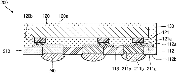
1. A method of forming an electronic component, comprising:
providing lands that are laterally separated by spaces, the lands comprising a conductor, land top surfaces, and land bottom surfaces opposite to the land top surfaces;
forming an insulator within the spaces, the insulator having an insulator top surface and an insulator bottom surface, the insulator top surface covering each of the land top surfaces, wherein:
the land bottom surfaces are exposed through the insulator bottom surface;
removing the insulator from the insulator top surface to expose the land top surfaces to provide a substrate having a substrate top surface adjacent to the land top surfaces and a substrate bottom surface adjacent to the land bottom surfaces;
depositing conductive patterns over the substrate top surface and coupled to the land top surfaces;
coupling an electronic device to the conductive patterns; and
forming a package body encapsulating the substrate top surface, at least portions of the electronic device, and at least portions of the conductive patterns,
wherein:
providing the lands comprises:
providing a work piece having a work piece top side and a work piece bottom side;
selectively removing portions of the work piece extending inward from the work piece top side to define the spaces; and
after forming the insulator and before removing the insulator from the insulator top surface:
first, globally removing a first portion of the work piece from the work piece bottom side; and
second, selectively removing a second portion of the work piece from the work piece bottom side to expose the insulator bottom surface and to define the land bottom surfaces.
|