| CPC H01L 23/13 (2013.01) [H01L 21/568 (2013.01); H01L 23/3185 (2013.01); H01L 23/49816 (2013.01); H01L 24/48 (2013.01); H01L 24/85 (2013.01); H01L 25/0657 (2013.01); H01L 25/18 (2013.01); H01L 2224/48145 (2013.01); H01L 2224/48157 (2013.01); H01L 2224/85005 (2013.01); H01L 2225/06506 (2013.01); H01L 2225/0651 (2013.01); H01L 2225/06562 (2013.01)] | 18 Claims |
|
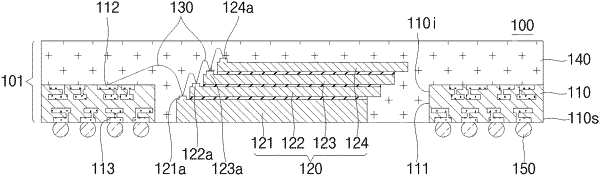
1. A semiconductor device, comprising:
a first module, comprising:
a first substrate comprising a first cavity and a first internal terminal;
a first device stack in the first cavity and comprising a plurality of electronic devices, wherein a first electronic device of the plurality of electronic devices comprises a first device terminal;
a first encapsulant in the first cavity and covering lateral sides of the plurality of electronic devices of the first device stack; and
a first internal interconnect in the first encapsulant and coupled with the first internal terminal and the first device terminal;
wherein:
the first substrate comprises a substrate shelf;
the first substrate comprises a substrate ledge portion and a substrate vertical portion extending from the substrate ledge portion, the substrate ledge portion including a ledge;
the substrate ledge portion defines a first width of the first cavity and the substrate vertical portion defines a second width of the first cavity greater than the first width of the first cavity; and
the substrate shelf comprises the ledge and the ledge includes the first internal terminal.
|