| CPC H01L 21/823814 (2013.01) [H01L 21/0337 (2013.01); H01L 21/28247 (2013.01); H01L 21/28568 (2013.01); H01L 21/3086 (2013.01); H01L 21/31105 (2013.01); H01L 21/31144 (2013.01); H01L 21/76224 (2013.01); H01L 21/76816 (2013.01); H01L 21/823431 (2013.01); H01L 21/823481 (2013.01); H01L 21/823807 (2013.01); H01L 21/823821 (2013.01); H01L 21/823842 (2013.01); H01L 21/823857 (2013.01); H01L 21/823871 (2013.01); H01L 21/823878 (2013.01); H01L 23/5226 (2013.01); H01L 23/5283 (2013.01); H01L 23/53238 (2013.01); H01L 23/53266 (2013.01); H01L 27/0924 (2013.01); H01L 28/24 (2013.01); H01L 29/0847 (2013.01); H01L 29/41791 (2013.01); H01L 29/516 (2013.01); H01L 29/6653 (2013.01); H01L 29/7843 (2013.01); H01L 29/7846 (2013.01); H01L 29/7854 (2013.01); H10B 10/12 (2023.02)] | 20 Claims |
|
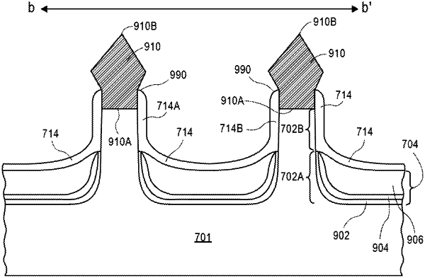
1. An integrated circuit structure, comprising:
a P-type semiconductor device above a substrate, the P-type semiconductor device comprising:
a first three-dimensional body comprising silicon;
a first gate dielectric layer over the first three-dimensional body;
a first gate electrode over the first gate dielectric layer, the first gate electrode completely around the first three-dimensional body, the first gate electrode having a first side and a second side opposite the first side;
first and second semiconductor source or drain regions adjacent the first and second sides of the first gate electrode, respectively;
first and second trench contact structures over the first and second semiconductor source or drain regions adjacent the first and second sides of the first gate electrode, respectively; and
a first metal silicide layer directly between the first and second trench contact structures and the first and second semiconductor source or drain regions, respectively; and
an N-type semiconductor device above the substrate, the N-type semiconductor device comprising:
a second three-dimensional body comprising silicon;
a second gate dielectric layer over the second three-dimensional body;
a second gate electrode over the second gate dielectric layer, the second gate electrode completely around the second three-dimensional body, the second gate electrode having a first side and a second side opposite the first side;
third and fourth semiconductor source or drain regions adjacent the first and second sides of the second gate electrode, respectively;
third and fourth trench contact structures over the third and fourth semiconductor source or drain regions adjacent the first and second sides of the second gate electrode, respectively; and
a second metal silicide layer directly between the third and fourth trench contact structures and the third and fourth semiconductor source or drain regions, respectively, wherein the first metal silicide layer comprises at least one metal species not included in the second metal silicide layer.
|