| CPC H01L 21/76807 (2013.01) [H01L 21/02019 (2013.01); H01L 21/02065 (2013.01); H01L 23/5226 (2013.01); H01L 23/528 (2013.01); H01L 27/14636 (2013.01); H10N 70/066 (2023.02); H01L 2224/80004 (2013.01)] | 5 Claims |
|
1. An interconnect structure for an integrated circuit comprising:
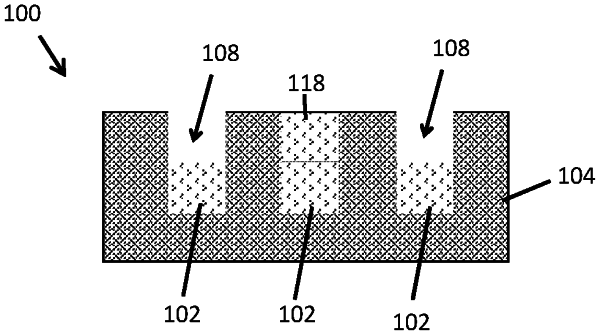
a wafer including a plurality of trenches, the wafer extending along a first axis to define a horizontal wafer length and a second axis orthogonal to the first axis to define a vertical wafer height;
a plurality of first-type interconnect elements embedded in the wafer, each of the first-type interconnect elements in a respective trench among the plurality trenches and directly contacting sidewalls of the respective trench, and each of the first-type interconnect elements extending along the first axis to define a first horizontal length and along the second axis to define a first vertical height;
a second-type interconnect element embedded in the wafer and in a corresponding trench among the plurality of trenches, the second-type of interconnect element directly contacting an underlying first-type interconnect element among the plurality of first-type interconnect elements and directly contacting sidewalls of the corresponding trench, the second-type interconnect element extending along the first axis to define a second horizontal length and along the second axis to define a second vertical height, the second horizontal length being substantially equal to the first horizontal length;
wherein the interconnect structure includes the second-type interconnect element that directly contacts the underlying first-type interconnect element, the second-type interconnect element and the first-type interconnect element defining a conductive via comprising a metal material extending continuously along the second axis from a base of the underlying first-type interconnect element and stopping at the upper surface of the second-type interconnect element,
wherein the plurality of first-type interconnect elements are formed from a single metal material, and the second-type interconnect element formed from a single metal material, and
wherein an upper surface of the wafer is completely and each of the respective trench containing the first-type of interconnect element is not completely filled such that it exposes an upper surface of the first-type of interconnect element,
wherein the second vertical height is greater than the first vertical height.
|