| CPC H01L 21/4853 (2013.01) [H01L 21/4857 (2013.01); H01L 21/486 (2013.01); H01L 23/145 (2013.01); H01L 23/49816 (2013.01); H01L 23/49822 (2013.01); H01L 23/49894 (2013.01); H01L 25/0655 (2013.01); H01L 2021/60022 (2013.01); H01L 23/147 (2013.01); H01L 23/15 (2013.01); H01L 23/3128 (2013.01); H01L 23/49827 (2013.01); H01L 24/13 (2013.01); H01L 24/16 (2013.01); H01L 24/32 (2013.01); H01L 24/73 (2013.01); H01L 24/81 (2013.01); H01L 24/83 (2013.01); H01L 24/92 (2013.01); H01L 2224/0401 (2013.01); H01L 2224/13082 (2013.01); H01L 2224/131 (2013.01); H01L 2224/13147 (2013.01); H01L 2224/16227 (2013.01); H01L 2224/32225 (2013.01); H01L 2224/73204 (2013.01); H01L 2224/81203 (2013.01); H01L 2224/81815 (2013.01); H01L 2224/83192 (2013.01); H01L 2224/92125 (2013.01); H01L 2924/1432 (2013.01); H01L 2924/1434 (2013.01); H01L 2924/15311 (2013.01); H01L 2924/181 (2013.01); H01L 2924/18161 (2013.01); H01L 2924/19105 (2013.01)] | 18 Claims |
|
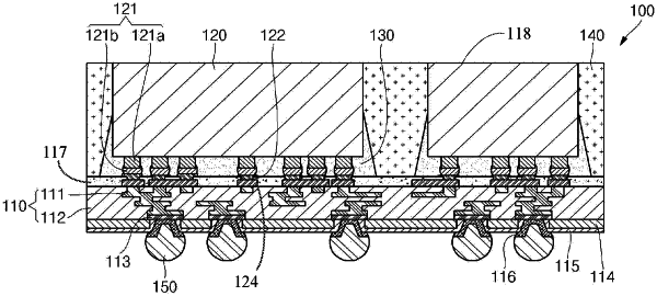
1. An electronic device comprising:
an under layer (UL) comprising a top UL side, a bottom UL side, and a UL aperture that extends between the top UL side and the bottom UL side;
an interposer comprising:
a bottom interposer side coupled to the top UL side, a top interposer side, and a lateral interposer side;
an interposer dielectric layer at the bottom interposer side; and
an interposer conductive layer at the bottom interposer side, wherein at least a portion of the interposer conductive layer is exposed through the under layer (UL) by the UL aperture;
an upper dielectric layer on the top interposer side;
an upper conductive layer on the top interposer side;
a lower signal distribution structure on the bottom UL side and configured to electrically couple an interconnection structure to a bottom side of the interposer conductive layer through the UL aperture;
a first semiconductor die electrically coupled to the interposer through the upper conductive layer, wherein the first semiconductor die vertically covers only a first portion of the interposer; and
a second semiconductor die electrically coupled to the interposer through the upper conductive layer, wherein the second semiconductor die vertically covers only a second portion of the interposer.
|